공통 · 2026-09-10
GPU Architecture: Compute Units and Memory
Explore SMs, CUDA Cores, Tensor Cores, and GPU memory, then connect capacity, bandwidth, and access latency to running a model.
In the previous article, we saw how a GPU distributes computation across many compute units, and why these units also need a supply of data to do their work. This time, we will look inside the GPU to understand where it computes and where it stores data. From there, we will explore which memory characteristics matter when running a model. We will use NVIDIA GPUs for this explanation.
From the GPU to the Inside of an SM
An NVIDIA GPU contains multiple SMs (Streaming Multiprocessors). Each SM schedules instructions and performs computation using its internal compute units. Let us take a closer look at the groups of compute units we drew in the previous article.
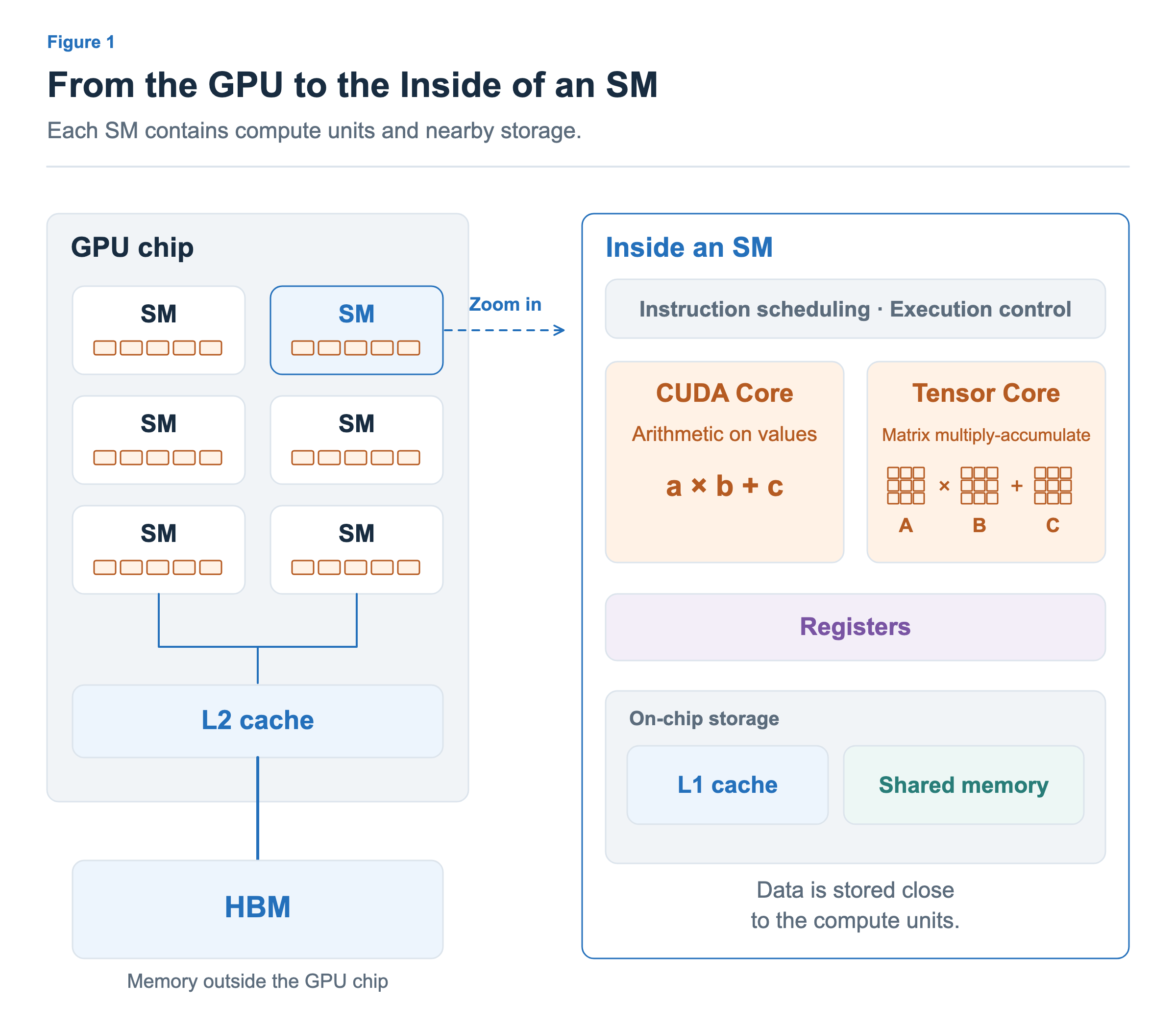
On the left of Figure 1, multiple SMs and an L2 cache sit inside the GPU chip, while HBM (High Bandwidth Memory) sits outside it. HBM holds data such as model weights and inputs. Each SM fetches the data it needs for computation, and the L2 cache supports memory access across the SMs. NVIDIA’s description of the Blackwell Ultra architecture also shows the arrangement of SMs, L2 cache, and HBM. Some GPUs connect two compute dies to operate as a single GPU, but our diagram focuses on the basic components.
The right side shows an enlarged SM. Instruction scheduling and execution control sit at the top, with CUDA Cores and Tensor Cores below. CUDA Cores perform arithmetic on individual values, such as addition, multiplication, and multiply-accumulate operations. In the diagram’s a × b + c, a, b, and c are each a single number. Tensor Cores specialize in multiplying and accumulating small matrix blocks. In the neighboring A × B + C, A, B, and C are matrices, and A × B is a matrix multiplication.
CUDA Cores can also compute matrix multiplications by executing the individual multiplications and additions that make them up. Tensor Cores process this regular computation in matrix blocks. The distinction is therefore not whether the units compute in parallel, but what form of computation they are designed to perform. Supported data types and matrix operation sizes vary by GPU generation.
Alongside the compute units, an SM contains spaces such as registers, L1 cache, and shared memory that keep data closer to the compute units. The diagram shows the relationships between these components, not their actual counts or relative areas. Next, let us examine how each space holds the values needed for computation.
Where Is Data Stored?
We cannot keep every model weight and every value being computed right beside the compute units. A GPU combines memory for large amounts of data with smaller storage spaces located closer to computation. Figure 2 places two SMs side by side to distinguish the spaces accessed by multiple SMs from those inside each SM.
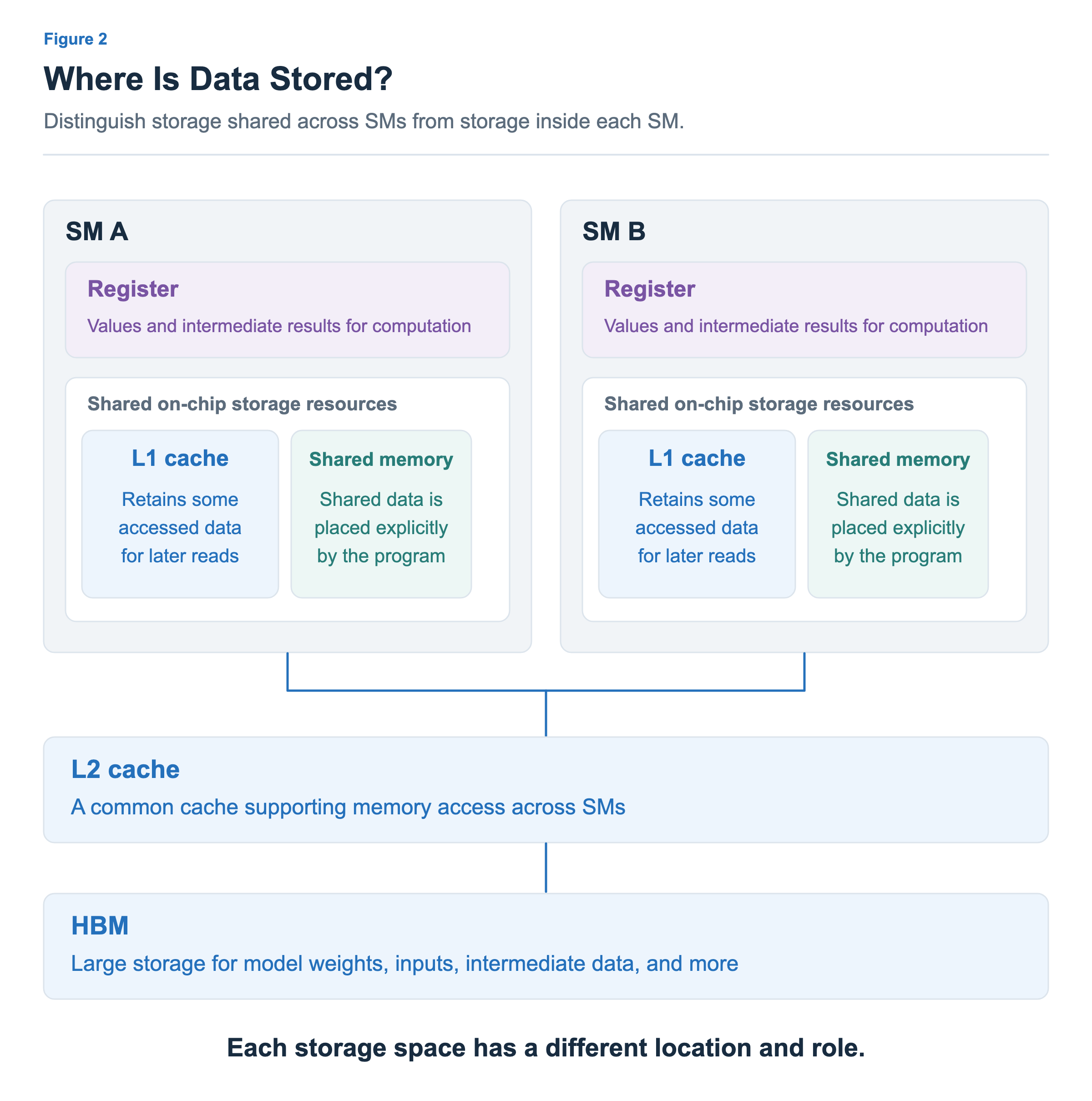
At the bottom, HBM is a large storage space for model weights, inputs, intermediate data, and more. Accesses to data stored in HBM can benefit from the L2 cache. A cache retains some of the data that has been accessed so it can be used again when needed. If the required data remains in L2, it can reduce the need to fetch that data from HBM again. Multiple SMs share the L2 cache, while each SM has its own L1 cache.
Shared memory is a storage space where developers can directly control data placement and reuse. For example, if several computations repeatedly use the same input values, a developer can write code that brings those values into shared memory and uses them together. Caches also help reuse data, but in ordinary cache operation, the hardware retains and replaces the data. With shared memory, developers can explicitly decide which data to bring in and when to reuse it.
We drew L1 cache and shared memory inside one border to represent the NVIDIA GPU design in which the two functions share storage resources on the GPU chip. Their physical resources are connected, but their roles in a program are different. NVIDIA’s CUDA guide lists the unified storage sizes and the capacities available to shared memory across GPU generations.
At the top, registers are small storage spaces for values and intermediate results used in individual computations. Compute units perform arithmetic on values prepared in registers and place the results back in registers for subsequent computation. Registers hold the values needed for active computation, rather than all the data stored in HBM.
Data does not have to pass through all these spaces in order. In particular, shared memory is a space used by explicitly placing data there, so it is not a mandatory step for every computation. The lines in Figure 2 show the locations of storage spaces and their access relationships.
How different are their actual sizes? The table below compares the spaces introduced above for a Blackwell B200 configuration with 148 SMs. The SM count comes from NVIDIA’s B200 platform specifications, and memory capacities come from the Blackwell guide. For spaces present in each SM, the GPU-wide totals are calculated by multiplying the per-SM capacity by 148.
| Storage space | Per SM | Across the GPU |
|---|---|---|
| Registers | 256 KiB | 37 MiB in total |
| Unified L1 cache / shared memory | 256 KiB | 37 MiB in total |
| ↳ L1 cache | Part of the unified 256 KiB; depends on the shared memory allocation | Part of the unified 37 MiB; depends on the allocation |
| ↳ Shared memory | Up to 228 KiB of the unified space | Up to about 33 MiB in total |
| L2 cache | Not allocated separately to each SM | 126 MB, shared across SMs |
| HBM | Not allocated separately to each SM | 180 GB |
A KiB is 1,024 bytes, and a MiB is 1,024 KiB. L2 and HBM retain the MB and GB notation used in NVIDIA’s documentation. L1 cache and shared memory are included in the unified space, so their capacities are not added separately. Likewise, having 37 MiB of registers across the GPU does not mean one SM can use all that space. It is the sum of capacities distributed across the SMs.
What matters in these numbers is the difference in scale. Storage close to the compute units is measured in hundreds of KiB per SM, while HBM holds hundreds of GB per GPU. The newer B300 offers 288 GB of HBM3e per GPU. This difference helps explain why a GPU keeps large model data in HBM and brings a portion of it closer to the compute units as needed.
What Happens When We Add Two Values?
Let us connect this structure to a simple computation. Suppose memory holds a = 2 and b = 3, and we want to add them and store c = 5 in memory. To focus on the flow of values, Figure 3 leaves out the details of caches and the units that move data.
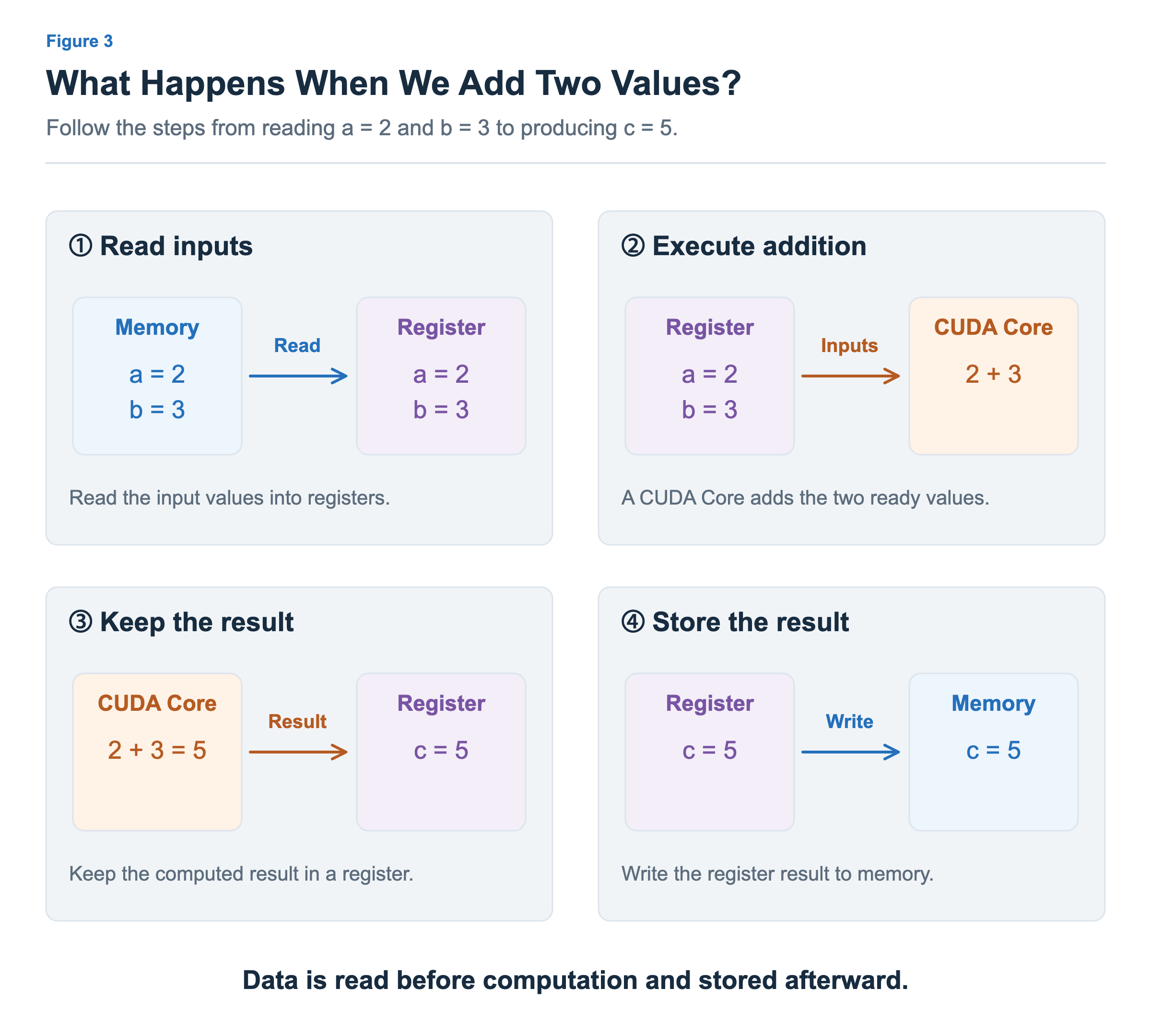
In ①, the inputs are read from memory and prepared in registers. Having inputs stored in GPU memory is different from having those values immediately available to the compute units. The required values must arrive before the computation can execute.
In ②, a CUDA Core adds the two prepared values. Executing the addition instruction places the result, 5, in a register as shown in ③. Reading the inputs, computing with the fetched values, and keeping the result are distinct parts of the process.
In ④, the result in the register is stored in memory. This example ends after storing the result, but if another computation follows, it may reuse the value in the register directly. A result does not have to be stored in HBM after every arithmetic operation.
Matrix multiplication in a model also involves reading many inputs and weights, performing multiplications and additions, and keeping the results. The amount of input data fetched and intermediate data stored depends on how the computation is organized. To understand GPU execution, we need to look at both the compute units’ arithmetic capability and the process of fetching the required data and storing results.
What to Look at in Memory When Running a Model
To run a model on a GPU, the model and the data needed for execution must first fit in memory. Once they fit, the required values must be supplied at a rate that keeps up with the compute units. There is also the time spent waiting for a requested value to arrive. Capacity, bandwidth, and access latency in Figure 4 help us understand these respective issues.
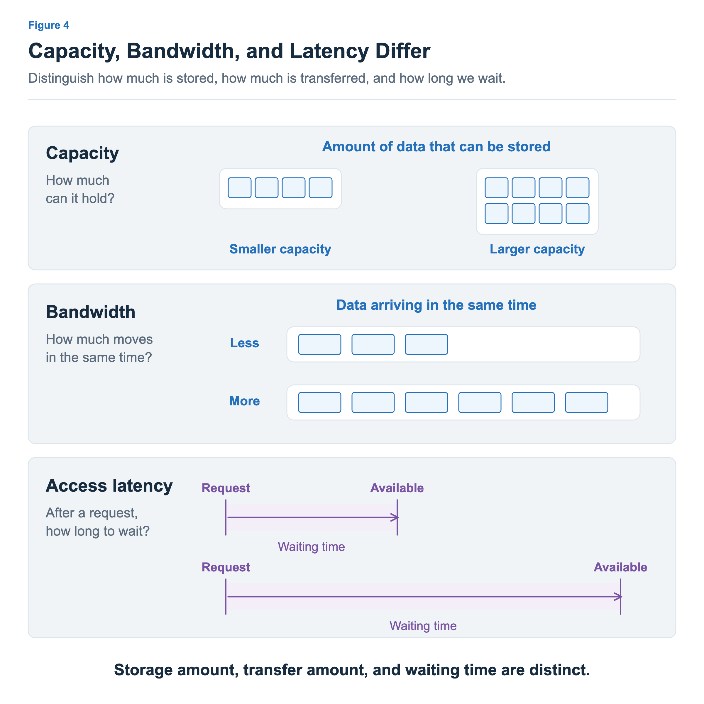
Even if we want to load a large model onto a GPU, insufficient memory can prevent us from storing all its weights. For example, 100 billion weights stored at 2 bytes each require about 200 GB just for the weights. Inputs and intermediate results need additional space. The first property to check here is capacity: the amount of data that can be stored. As in the first panel, a larger capacity holds more data, but fitting the data does not by itself make computation fast.
Even when a model fits in memory, many compute units need a sufficient supply of inputs and weights to keep working. If data arrives too slowly relative to what the units can process, we cannot fully use their computing capability. The relevant property is bandwidth: the amount of data that can be transferred per unit of time. It is usually expressed in GB/s or TB/s. As in the second panel, higher bandwidth means more data arrives in the same time. Insufficient bandwidth relative to the required data movement can limit execution speed. How much of a product’s specified peak bandwidth is actually used also depends on memory access patterns and execution conditions.
Can we then divide the size of the data to fetch by bandwidth to find how long we must wait before computation can start? That calculation helps estimate the time needed to transfer a large amount of data, but it does not fully explain the waiting time for one request. The steps involved differ depending on whether the required value is in a cache or must be read from HBM. Preparing a read inside memory takes time, and a request may also have to wait for other requests to be processed. The time until data arrives is not determined by data size and bandwidth alone. NVIDIA’s memory research also considers request queues and accesses within DRAM together.
The time from requesting data until it can be used is called memory access latency. The third panel shows how long an individual request waits. In our earlier addition example, if even one input has not arrived, the addition cannot execute. Even when the requested amount of data is small, waiting for that value can delay the computation.
When multiple requests overlap, data can keep arriving even though each request has a waiting time. In this case, the total amount of data transferred over a period may be large, without each request’s latency becoming correspondingly short. Bandwidth describes the amount of data supplied through multiple requests, while access latency describes the waiting time of each request. The two can influence each other, but they do not mean the same thing.
When looking at GPU memory, we therefore need to distinguish whether it has enough capacity for the required data, whether it can keep delivering sufficient amounts of data, and how long each requested value takes to arrive. Even with many compute units, a computation that uses a value cannot proceed until that value arrives.
In this article, we explored the compute units and storage spaces inside a GPU, along with the flow of reading data, computing, and storing results. In the next article, we will revisit element-wise operations, reductions, and matrix multiplication to examine which computations can proceed together and where results must be brought together.